EV32C6A3A1-24.576M TR 数据手册
EV32C6 Series
REGULATORY COMPLIANCE
2011/65 +
2015/863
191 SVHC
ITEM DESCRIPTION
Voltage Controlled Quartz Crystal Clock Oscillators VCXO LVCMOS/TTL (CMOS) 3.3Vdc 6 Pad 5.0mm x 7.0mm Ceramic Surface
Mount (SMD)
ELECTRICAL SPECIFICATIONS
Nominal Frequency
1.544MHz to 77.76MHz
Frequency Tolerance/Stability
Inclusive of all conditions: Calibration Tolerance at 25°C, Frequency Stability over the Operating Temperature Range,
Supply Voltage Change, Output Load Change, Shock, and Vibration.
±50ppm Maximum
Aging at 25°C
±2ppm/First Year Typical, ±10ppm/10 Years Maximum
Operating Temperature Range
Supply Voltage
0°C to +70°C
-40°C to +85°C
3.3Vdc ±10%
Input Current
15mA Maximum
Output Voltage Logic High (VOH)
IOH = -4mA
90% of Vdd Minimum
Output Voltage Logic Low (VOL)
IOL = +4mA
10% of Vdd Maximum
Measured at 20% to 80% of Waveform
5nSec Maximum
Measured at 50% of Waveform
50 ±10(%)
10TTL Load or 30pF LVCMOS Load Maximum over Nominal Frequency of 1.544MHz to 12.288MHz
15pF LVCMOS Load Maximum over Nominal Frequency of 12.288001MHz to 77.76MHz
CMOS
Rise/Fall Time
Duty Cycle
Load Drive Capability
Output Logic Type
Absolute Pull Range
Control Voltage Range
Inclusive of all conditions: Calibration Tolerance at 25°C, Frequency Stability over the Operating Temperature Range,
Supply Voltage Change, Output Load Change, Shock, Vibration, and Aging over the Control Voltage (Vc).
±50ppm Minimum
±80ppm Minimum (Only available over Nominal Frequency range of 1.544MHz to 51.84MHz)
±100ppm Minimum (Only available over Nominal Frequency range of 1.544MHz to 36MHz)
Test Condition for APR
0.3Vdc to 3.0Vdc
0.0Vdc to Vdd
Control Voltage
Linearity
10% Typical, 20% Maximum
Transfer Function
Positive Transfer Characteristic
Modulation Bandwidth
Input Impedance
Measured at -3dB, Vc = 1.65Vdc
10kHz Minimum
50kOhms Minimum
Input Leakage Current
10µA Maximum
Phase Noise
All Values are Typical
-70dBc/Hz at offset of 10Hz
-100dBc/Hz at offset of 100Hz
-130dBc/Hz at offset of 1kHz
-147dBc/Hz at offset of 10kHz
-152dBc/Hz at offset of 100kHz
-155dBc/Hz at offset of 1MHz
Tri-State Input Voltage (Vih and Vil)
90% of Vdd Minimum or No Connect to Enable Output,
10% of Vdd Maximum to Disable Output (High Impedance)
Fj = 12kHz to 20MHz; Random
1pSec Maximum
RMS Phase Jitter
Revised N: 4/14/2014
Page 1 of 9
www.ecliptek.com
�EV32C6 Series
Start Up Time
10mSec Maximum
Storage Temperature Range
-55°C to +125°C
PART NUMBERING GUIDE
ENVIRONMENTAL & MECHANICAL SPECIFICATIONS
ESD Susceptibility
MIL-STD-883, Method 3015, Class 1, HBM: 1500V
Fine Leak Test
MIL-STD-883, Method 1014, Condition A
Flammability
UL94-V0
Gross Leak Test
MIL-STD-883, Method 1014, Condition C
Mechanical Shock
MIL-STD-883, Method 2002, Condition B
Moisture Resistance
MIL-STD-883, Method 1004
Moisture Sensitivity
J-STD-020, MSL 1
Resistance to Soldering Heat
MIL-STD-202, Method 210, Condition K
Resistance to Solvents
MIL-STD-202, Method 215
Solderability
MIL-STD-883, Method 2003
Temperature Cycling
MIL-STD-883, Method 1010, Condition B
Vibration
MIL-STD-883, Method 2007, Condition A
Revised N: 4/14/2014
Page 2 of 9
www.ecliptek.com
�EV32C6 Series
MECHANICAL DIMENSIONS
SUGGESTED SOLDER PAD LAYOUT
PIN
1
CONNECTION
Control Voltage
2
Tri-State
3
Case Ground
4
Output
5
No Connect
6
Supply Voltage
All Tolerances are ±0.1
All Dimensions in Millimeters
Revised N: 4/14/2014
Page 3 of 9
www.ecliptek.com
�EV32C6 Series
OUTPUT WAVEFORM & TIMING DIAGRAM
Revised N: 4/14/2014
Page 4 of 9
www.ecliptek.com
�EV32C6 Series
TEST CIRCUIT FOR CMOS OUTPUT
Note 1: An external 0.01µF ceramic bypass capacitor in parallel with a 0.1µF high frequency ceramic bypass capacitor close (less
Than 2mm) to the package ground and supply voltage pin is required.
Note 2: A low capacitance (10Mohms), and high bandwidth (>300MHz) passive
Probe is recommended.
Note 3: Capacitance value CL includes sum of all probe and fixture capacitance.
Revised N: 4/14/2014
Page 5 of 9
www.ecliptek.com
�EV32C6 Series
TEST CIRCUIT FOR TTL OUTPUT
Note 1: An external 0.01µF ceramic bypass capacitor in parallel with a 0.1µF high frequency ceramic bypass capacitor close (less
Than 2mm) to the package ground and supply voltage pin is required.
Note 2: A low capacitance (10Mohms), and high bandwidth (>300MHz) passive
Probe is recommended.
Note 3: Capacitance value CL includes sum of all probe and fixture capacitance.
Note 4: Resistance value RL is shown in Table 1. See applicable specification sheet for 'Load Drive Capability'.
Note 5: All diodes are MMBD7000, MMBD914, or equivalent.
Revised N: 4/14/2014
Page 6 of 9
www.ecliptek.com
�EV32C6 Series
TAPE & REEL DIMENSIONS
Quantity per Reel: 1,000 Units
All Dimensions in Millimeters
Compliant to EIA-481
Revised N: 4/14/2014
Page 7 of 9
www.ecliptek.com
�EV32C6 Series
RECOMMENDED SOLDER REFLOW METHOD
HIGH TEMPERATURE INFRARED/CONVECTION
TS MAX to TL (Ramp-up Rate)
3°C/Second Maximum
Preheat
- Temperature Minimum (TS MIN)
- Temperature Typical (TS TYP)
- Temperature Maximum(TS MAX)
- Time (ts MIN)
150°C
175°C
200°C
60 - 180 Seconds
Ramp-up Rate (TL to TP)
3°C/Second Maximum
Time Maintained Above:
- Temperature (TL)
- Time (tL)
217°C
60 - 150 Seconds
Peak Temperature (TP)
260°C Maximum for 10 Seconds Maximum
Target Peak Temperature(TP Target)
250°C +0/-5°C
Time within 5°C of actual peak (tp)
20 - 40 Seconds
Ramp-down Rate
6°C/Second Maximum
Time 25°C to Peak Temperature (t)
8 Minutes Maximum
Moisture Sensitivity Level
Level 1
Additional Notes
Temperatures shown are applied to body of device.
High Temperature Manual Soldering
260°C Maximum for 5 Seconds Maximum, 2 times Maximum. (Temperatures shown are applied to body of device.)
Revised N: 4/14/2014
Page 8 of 9
www.ecliptek.com
�EV32C6 Series
RECOMMENDED SOLDER REFLOW METHOD
LOW TEMPERATURE INFRARED/CONVECTION
TS MAX to TL (Ramp-up Rate)
5°C/Second Maximum
Preheat
- Temperature Minimum (TS MIN)
- Temperature Typical (TS TYP)
- Temperature Maximum(TS MAX)
- Time (tS MIN)
N/A
150°C
N/A
60 - 120 Seconds
Ramp-up Rate (TL to TP)
5°C/Second Maximum
Time Maintained Above:
- Temperature (TL)
- Time (tL)
150°C
200 Seconds Maximum
Peak Temperature (TP)
240°C Maximum
Target Peak Temperature(TP Target)
240°C Maximum 2 Times/230˚C Maximum 1Time
Time within 5°C of actual peak (tP)
10 Seconds Maximum 2 Times / 80 Seconds Maximum 1 Time
Ramp-down Rate
5°C/Second Maximum
Time 25°C to Peak Temperature (t)
N/A
Moisture Sensitivity Level
Level 1
Additional Notes
Temperatures shown are applied to body of device.
Low Temperature Manual Soldering
185°C Maximum for 10 Seconds Maximum, 2 times Maximum. (Temperatures shown are applied to body of device.)
Revised N: 4/14/2014
Page 9 of 9
www.ecliptek.com
�
EV32C6A3A1-24.576M TR 价格&库存
很抱歉,暂时无法提供与“EV32C6A3A1-24.576M TR”相匹配的价格&库存,您可以联系我们找货
免费人工找货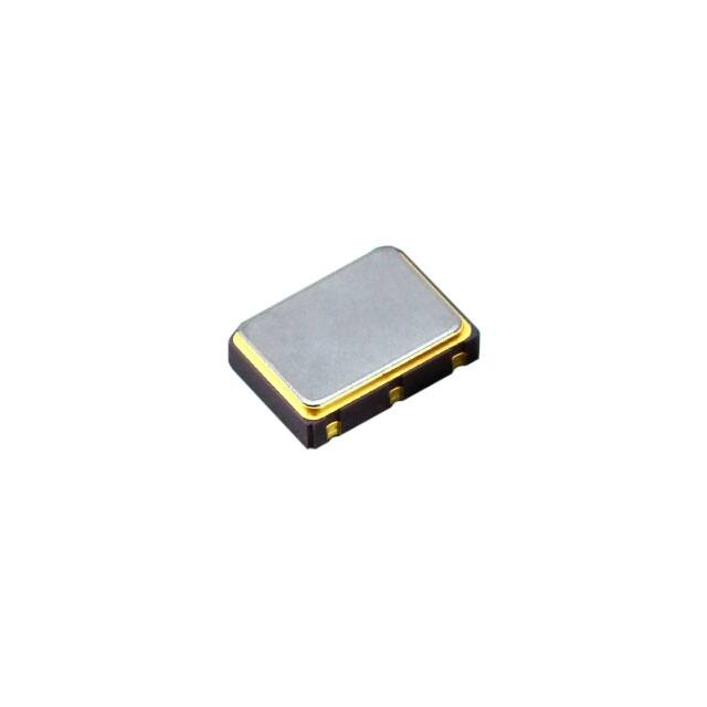


 工商网监
湘ICP备2023018690号
工商网监
湘ICP备2023018690号
